


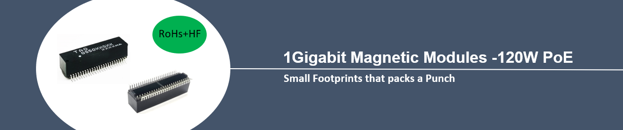
Network Card/Motherboard Design Guidelines..
Network Card/Motherboard Design Guidelines1 Introduction
This section provides information on 10/100BASE-T network cards and LAN motherboards for interest (LOM = LAN on)
Motherboard) Design information and special considerations.
2 element layout
The reasons for the importance of component location are:
Proper placement of components will reduce the possibility of problems directly related to electromagnetic interference (EMI).
The overall arrangement of components of LAN subsystems can simplify the layout of lines. Particular attention should be paid to the direction of components in circuit board design. Because the direction of components will determine the complexity of line layout to a certain extent. The aim is to minimize the crossing between bends and lines.
Correct design is also helpful for small pin foot complete LAN subsystem. It is important to minimize the space required for the entire subsystem, as it will eventually compete for space near the valuable motherboard connectors. For most subsystems, LAN circuits need to be close to connectors (RJ-45), so they must be optimized so that they can be arranged in very small spaces.
Distribution management is also an area requiring special care. Digital ground wire, analog ground wire and power supply board should be carefully placed to reduce voltage electromagnetic compatibility (EMC) problems.
3 magnetic field
This section describes the principles of magnetic field considerations, as it involves the design of network interface cards/LAN motherboards.
Components with magnetic fields (relays, inductors, transformers, etc.) should be separated or their magnetic rings should be at right angles to each other. this
Doing so will reduce the possibility of magnetic fields interfering with each other. The distance between them should be determined according to the intensity of the magnetic field and the signal. In order to prevent excessive noise coupling to network signals, do not close the network subsystem to the CPU. This is a good example of distance determination. Reducing the distance between the signal source and the equipment will shorten the line. These lines directly affect the size of EMI.
4 key dimensions
Two key dimensions must be considered when laying out physical layer chip (PHY), magnetic device and RJ45 connector.
4.1 Magnetic Device-RJ45
The key dimensions are shown in Figure 24. When arranging PCB, the most important thing to pay attention to is to reduce the distance A. The distance between the magnetic device and RJ-45 interface should be less than 1 inch. If A must be greater than an inch, the following two characteristics of the two lines are important:
(1) Characteristic impedance: The high frequency impedance of the signal line should be as close as possible to 50_.
(2) Line symmetry: the path of difference pairs (i.e. TX + and TX-) should be the same, and the length should be exactly the same.
Note: It is more important that the length of lines between devices is equal than the path of lines is completely symmetrical.
4.2 Physical Layer Chip (PHY) - Between Magnetic Devices
The key size B between devices in Figure 24 should also be less than one inch. Because high-speed signals are propagating along these lines,
Particular attention should be paid to the loss in the path between devices. In general, any path segment used for high-speed signals should be observed.
Unique terminal rules.
The unique terminal of the signal can reduce the reflection caused by the impedance mismatch between the device and the line. The high frequency components contained in the reflected signal may contribute more to EMI than the original signal itself. For this reason, the characteristic impedance of these lines should be designed as 50_+5%.
Notes for 5.0 Routes
Designers should pay close attention to minimizing crosstalk and propagation delay between parts of PCB that transmit high-speed signals.
Ring.
Geometric shape of 5.1 lines
The key factors to control the radiation of a line are the length and width of the line and the ratio of the line height to the ground plate height. in order to
To minimize the lead inductance, the clock and other high-speed lines should be shortened and widened as much as possible. In the signal layer, they should be close to the ground line.
Board (or power board). As shown in Figure 25, the above ratio is ideal between 1:1 and 1:3.
5.2 lines length
Keep the line length less than 1/20 of the maximum harmonic wavelength of the concerned frequency. Beyond this length, the line begins to look like an antenna, increasing
Add radiation. The line between decoupling line and input/output (I/O) filter capacitor should be very short. The inductance of long lines will drop
Low decoupling capacitor efficiency. For the same reason, the lines to the input/output signals and terminals should be as short as possible.
5.3 signal isolation
If possible, separate signals of the same type into separate layers. Putting all the clock-line related devices together can reduce the length of the line and radiation. Isolating input/output (I/O) signals from high-speed signals can control crosstalk that increases radiation and susceptibility. Avoid high-speed LAN lines that are close to other high-frequency signal devices (such as video controllers, caches, or CPUs).
5.4 Power Supply and Connection
Unless specified equipment manufacturer or specific design requirements (i.e. remote control exciter), all Vcc pins should be
Connecting to the same power supply, all Vss pins should be connected to the ground board. For high-speed signals, they should be as short as possible.
It may be directly connected to a common reference ground panel.
Note: It is important to connect the power supply and the ground floor according to the chip design proposal. Do not put power or ground pins together unless specified in the standard design.
5.5 Hidden High Speed Lines
Hide all the fast rising and falling time signal lines and clock signal lines between the power supply and the ground panel. Hidden layer
Fast lines between them can reduce the electromagnetic interference produced by these lines. In the outer layer, it is difficult to obtain the required line impedance, which is also the case.
It will directly affect the characteristics of echo loss.
5.6 Cross High Speed Signal Line
If a fast signal line must pass through